
Thermal Management in Heterogeneous Integration: Embedded Microfluidic Cooling Solutions
Anyone who has opened a laptop after a long gaming session knows that heat is the silent enemy of electronics. Now imagine that same problem in a package holding multiple high-power chiplets, stacked dies, and dense memory, all squeezed into a few square centimeters. That is the world of heterogeneous integration—and it is brutally hot. Traditional cooling methods are being pushed to their limits, and that is where embedded microfluidic cooling starts to sound less like a futuristic research topic and more like a practical necessity.
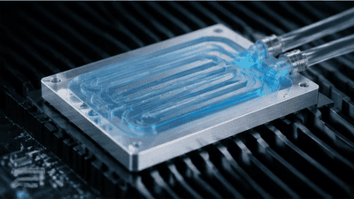
In this post, we explore how thermal management is changing as we move deeper into 2.5D and 3D heterogeneous integration, and why embedded microfluidic cooling solutions are attracting so much attention. Think of it as plumbing meets silicon: tiny channels, smart manifolds, and carefully tuned fluids, all built right into or around the chips themselves.
The Heat Problem in Heterogeneous Integration
Heterogeneous integration is about cramming more functionality into less space by combining different chips—CPU, GPU, AI accelerators, memory, RF, power, sensors—into a single system-in-package. This approach solves many architectural challenges but introduces a nasty thermal twist:
- Power densities go up as dies are stacked vertically and placed closer together.
- Hotspots become more concentrated and harder to reach from the outside.
- Heat must travel through more layers of materials—TIMs, underfill, interposers, substrates—before it escapes.
In 2.5D systems, the main logic sometimes sits in the middle of a “castle” of HBM stacks, radiating heat into a crowded neighborhood. In 3D ICs, the top dies can be partially insulated from external coolers by lower dies and interconnect layers. The result is a complex thermal landscape where a few square millimeters can become reliability nightmares if not cooled effectively.
Standard approaches—heat spreaders, thermal interface materials, and cold plates—still have a role, but they struggle to handle kilowatt-class power in compact, stacked packages without large temperature gradients. That is where embedded cooling comes in, quite literally, from the inside out.
What Is Embedded Microfluidic Cooling?
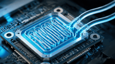
Embedded microfluidic cooling replaces the traditional idea of cooling from the outside with cooling from within. Instead of just attaching a cold plate on top of the package, tiny fluid channels—microchannels—are integrated directly into:
- The silicon die itself.
- The interposer or 2.5D substrate.
- A thin silicon cold plate bonded very close to the active layers.
Coolant flows through these channels, picking up heat at the point of generation. By minimizing the thermal distance between the hot transistor and the coolant, you dramatically lower thermal resistance and can sustain much higher power densities without exceeding safe junction temperatures.
The basic idea is simple: if heat is generated inside the silicon, why not put the coolant just a few microns away instead of a few millimeters? The execution, of course, is anything but simple, involving:
- Micromachining channels in silicon or other materials.
- Designing manifolds that distribute flow evenly.
- Choosing coolants that balance thermal performance, compatibility, and reliability.
Still, the concept is appealing because it attacks the thermal problem where it is hardest: at the source, inside the heterogeneous package.
Why Traditional Cooling Is Not Enough Anymore
It is worth pausing to ask: do we really need all this complexity? What is wrong with a well-designed cold plate, a couple of heat pipes, and a beefy fan?
In many systems, nothing is wrong. For CPUs, GPUs, and moderate-power 2.5D packages, carefully engineered cold plates and heat spreaders work fine. The trouble begins when:
- Power density exceeds what conventional solutions can handle without huge temperature rises.
- The package height and footprint are constrained, as in advanced servers or compact AI accelerators.
- Future roadmaps demand even higher power within similar or smaller form factors.
Traditional solutions suffer from multiple thermal interfaces—chip to TIM, TIM to heat spreader, spreader to cold plate—each contributing extra resistance. They also rely on heat traveling laterally through materials before it meets the coolant, creating hotspots. Embedded microfluidics, by contrast, tries to remove interfaces and shorten paths.
As heterogeneous integration pushes packages toward 3D stacks and more complex floorplans, the “bolt a better cooler on top” approach stops scaling. You need the cooling logic to be part of the package design, not an afterthought.
Embedded Microchannels: Variants and Architectures

Embedded microfluidic cooling is not a single technique; it is a family of approaches. Let’s walk through some of the more interesting architectural flavors.
1. Silicon-Embedded Microchannels
One common approach is to etch microchannels directly into a silicon layer—either the active die or a dedicated silicon cooling plate bonded to it. The channels might be:
- Straight, parallel channels under the entire die area.
- Hierarchical networks that branch like arteries and capillaries.
- Manifolded structures that distribute flow through specific hot regions.
These channels are then sealed with another wafer or cap layer, forming a network of sealed fluid paths running right beneath or above the active circuitry. Coolant is pumped in through inlets at the package edge and out through outlets, carrying heat away.
The key strength here is uniformity: with the right design, you can keep temperature variations across the die within a small range, which matters for timing, reliability, and device lifetime.
2. Interposer-Level Microfluidics
In 2.5D heterogeneous integration, logic and memory sit on a silicon interposer. This interposer is often underutilized from a thermal perspective. Embedding microchannels into the interposer layer offers an intriguing option:
- Channels can run beneath the logic die, HBM stacks, or both.
- Coolant pathways can be shared across multiple chiplets or tailored to their specific power maps.
- Thermal and electrical design can be co-optimized at the interposer level.
This arrangement is attractive because it avoids direct modification of complex logic dies while still placing cooling very close to them. It also aligns with the trend of using interposers as “integration platforms” not only for signals but now for thermal management as well.
3. Embedded Cold Plates and Hybrid Concepts
Another variation uses thin silicon or metal cold plates with embedded channels, bonded close to the die surfaces. These plates may:
- Replace or augment traditional heat spreaders.
- Be stacked in 3D with dies, forming alternating layers of logic and cooling.
- Serve as both mechanical stiffeners and thermal conduits.
This hybrid approach is often easier to introduce into existing packaging flows than full-on “cooling inside the active die,” while still delivering much lower thermal resistance than a distant cold plate.
Designing Microfluidics Around Hotspots
One of the more interesting shifts in thinking is that cooling design is becoming as “chip-aware” as the logic design itself. For embedded microfluidics to shine in heterogeneous integration, engineers must:
- Know where hotspots are: AI cores, cache blocks, transceiver clusters, power devices.
- Understand how workloads move hotspots around over time.
- Map power density patterns onto channel layouts and flow rates.
Straight, evenly spaced channels tend to be an okay starting point but rarely optimal. More advanced designs use:
- Topology optimization algorithms to shape channels around high-power regions.
- Hierarchical networks mimicking biological systems—arteries, veins, capillaries—to balance pressure drop and heat removal.
- Variable cross-sections and branch densities that tune cooling intensity locally.
The resulting microfluidic networks often look organic and irregular rather than grid-like. That’s a sign that the cooling is being designed around the actual needs of the chip, not around manufacturing convenience alone.
Coolants, Materials, and Reliability

Putting liquids inside or very near to active silicon sounds risky—and it is if not done carefully. Reliability and materials compatibility become central concerns. Some of the factors designers wrestle with include:
- Coolant choice. Water is a great thermal medium but can corrode or interact with certain metals. Specialized dielectric fluids avoid electrical issues but may have lower heat capacity or higher cost.
- Electrochemical stability. When metals and electrolytes share close quarters, you must prevent galvanic reactions and long-term degradation.
- Mechanical stress. Microchannels introduce new structures and interfaces. Thermal cycling can cause stress concentration if materials are not matched well.
- Leak prevention. Bonding quality, seal design, and fault-tolerant layouts are crucial; a leak inside a package is the ultimate nightmare.
Engineers balance all this against performance gains. In many cases, embedded microfluidic cooling allows junction temperatures to drop by tens of degrees Celsius, enabling higher clock speeds, more cores, or simply safer operation. Those benefits must outweigh the added manufacturing complexity and reliability risk for the solution to make sense in production.
Integration with Advanced Encapsulation and Packaging
Thermal design does not live in isolation; it is deeply intertwined with advanced encapsulation and heterogeneous integration flows. Embedding microfluidic cooling changes how you think about:
- Package stack-up and materials: mold compounds, substrates, and interposers all need to work harmoniously with the cooling layers.
- Assembly processes: bonding microchannel layers, aligning inlets and outlets, and sealing interfaces become new steps in the packaging line.
- Mechanical support: carriers and lids must protect fragile microfluidic structures during handling and operation.
In a chiplet-based system, for example, some dies may sit on an interposer with embedded channels, while others rely on conventional conduction to a common cold plate. Yet others—like high-power RF or GaN power devices—might have their own localized microfluidic loops. The package becomes a multi-modal cooling system where different elements use different thermal strategies, all wrapped in one encapsulated module.
That means advanced encapsulation engineers now play a key role in thermal innovation. They are no longer just “packaging” the chip; they are co-architects of its cooling and reliability story.
System-Level Implications: Data Centers and Beyond
Embedded microfluidic cooling is not just a cool trick at the chip level; it has system-level implications, especially in data centers and high-performance computing systems.
By removing heat more efficiently at the package level, you can:
- Raise coolant inlet temperatures, which improves chiller efficiency and enables more use of “free cooling.”
- Reduce the need for bulky cold plates, heat pipes, or extremely aggressive airflow.
- Increase rack density by packing more compute into the same footprint without cooking the hardware.
In other domains—like telecom, automotive, and aerospace—embedded cooling can help keep compact, sealed systems within safe temperatures under harsh environmental conditions. For instance, a heterogeneous module inside an electric vehicle might include power electronics, AI, and sensors all in a tight space. Microfluidic channels integrated in the package can tie directly into the vehicle’s coolant loop, improving overall thermal efficiency.
Challenges and Open Questions
For all its promise, embedded microfluidic cooling is not yet the default choice, and that is largely because a list of open questions and challenges remains:
- Manufacturing cost. Etching microchannels, bonding layers, and adding fluid interfaces all add cost and complexity to the manufacturing flow.
- Standardization. Every chip and package has its own ideal microfluidic layout; standardizing enough for scalable production is hard.
- Inspection and test. How do you test for leaks, blockages, or defects in embedded channels at scale without destroying the package?
- Serviceability. If a microfluidic path fails in the field, replacement is not as simple as swapping a fan or a cold plate.
These are not insurmountable roadblocks, but they do mean that embedded microfluidics will likely appear first where power densities and system constraints are most extreme—flagship AI accelerators, high-end HPC modules, specialized power devices—before trickling down into more mainstream applications.
Designing for the Future: Co-Engineering Silicon, Cooling, and Package
Perhaps the biggest conceptual shift in all of this is that thermal management in heterogeneous integration is no longer something you bolt on at the end. Instead, you design:
- Silicon floorplans with thermal-aware mapping of blocks and hotspots.
- Microfluidic networks co-optimized with power distribution and signal routing.
- Packages that support not only electrical and mechanical needs but also the plumbing of embedded cooling.
This co-engineering mindset brings device designers, thermal engineers, packaging experts, and even system architects into the same room. It also opens new optimization spaces: maybe you accept a slightly larger die if it simplifies channel layout and lowers peak temperature, or you rearrange chiplets on an interposer to minimize both routing congestion and cooling complexity.
In the long run, embedded microfluidic cooling could become as integral to heterogeneous integration roadmaps as through-silicon vias or chiplet interconnect standards. When that happens, “thermal design” stops being a constraint and becomes a design dimension in its own right.
Conclusion: Cooling from the Inside Out
Thermal management in heterogeneous integration is no longer just about heat sinks and fans. It is about how cleverly you can bring cooling into the heart of the package, right next to the transistors that are doing the hard work. Embedded microfluidic cooling is one of the most promising ways to do that, especially as power densities climb and traditional methods reach their limits.
There is still a long way to go—issues of cost, reliability, manufacturing, and standardization remain. But the direction of travel is clear. As 2.5D and 3D systems pack more diverse dies into ever tighter spaces, the industry is moving from cooling “around” the chip to cooling “through” it. In that world, microchannels and manifolds etched into silicon may be as important as the cores and cache they are cooling, and thermal management becomes a core part of what it means to design advanced, heterogeneous systems.





